Thursday, March 31, 2016

8051 DC Motor Interfacing

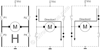
A direct current (DC) motor is used to translate electrical pulses into mechanical movement. In the DC motor we have only + and – leads. Connecting them to a DC voltage source moves the motor in one direction. By reversing the polarity, the DC motor will move in the opposite direction. With the help of relays or some specially designed chips we can change the direction of the DC motor rotation. H-Bridge concept can be used to control the direction of DC motor.

8051 DC Motor Interfacing

H-Bridge Logic Configurations:
Motor Operation P1 P2 P3 P4
Off Open Open Open Open
Clockwise Closed Open Open Closed
Counter Clockwise Open Open Closed Closed
Invalid Closed Closed Closed Closed

Program to move DC motor clockwise and counter clockwise.

ORG 0H
MAIN: CLR P1.0 ; P1
CLR P1.1 ; P2
CLR P1.2 ; P3
CLR P1.3 ; P4
SETB P2.7
MONITOR: JNB P2.7, CLOCKWISE
SETB P1.0 ; P1
CLR P1.1 ; P2
CLR P1.2 ; P3
SETB P1.3 ; P4
SJMP MONITOR
CLOCKWISE: CLR P1.0 ; P1
SETB P1.1 ; P2
SETB P1.2 ; P3
CLR P1.3 ; P4
SJMP MONITOR
END


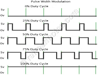
By changing the width of the pulse applied to the DC motor we can increase or decrease the amount of power provided to the motor, thereby increasing or decreasing the motor speed. Although the voltage has fixed amplitude, it has a variable duty cycle. That means the wider the pulse, the higher the speed. We can create the various duty cycle pulses using software.

8051 DC Motor Interfacing - PWM

Program to generate pulse of different duty cycle.
ORG 0H
MAIN:
CLR P1.0
SETB P2.7
MONITOR:
JNB P2.7, FIFTYPERCENT
SETB P1.0 ; high pulse
MOV R5, #25
ACALL DELAY
CLR P1.0 ; low pulse
MOV R5, #75
ACALL DELAY
SJMP MONITOR
FIFTYPERCENT:
SETB P1.0
MOV R5, #50 ; high pulse
ACALL DELAY
CLR P1.0 ; low pulse
MOV R5, #50
ACALL DELAY
SJMP MONITOR
DELAY:
HERE1: MOV R2, #100
HERE2: MOV R3, #255
HERE3: DJNZ R3, HERE3
DJNZ R2, HERE2
DJNZ R5, HERE1
RET
END


Related topics:
8051 External Program Memory Interfacing   |   8051 External Data Memory Interfacing   |   8051 Memory Mapped IO   |   8051 LED Interfacing   |   8051 Switch Interfacing   |   8051 Keyboard Interfacing   |   8051 7-Segment Display Interfacing   |   8051 LCD Interfacing   |   8051 ADC Interfacing   |   8051 DAC Interfacing   |   8051 Relay Interfacing   |   8051 Sensor Interfacing   |   8051 Stepper Motor Interfacing

List of topics: 8051
8051 Stepper Motor Interfacing

A stepper motor is a widely used device that translates electrical pulses into mechanical movement. Stepper motors commonly have a permanent magnet rotor (also called the shaft) surrounded by a stator. The most common stepper motors have four stator windings that are paired with a center-tapped common. This type of stepper motor is commonly referred to as a four-phase or unipolar stepper motor. The center tap allows a change of current direction in each of two coils when a winding is grounded, thereby resulting in a polarity change of the stator. As the sequence of power is applied to each stator winding, the rotor will rotate. There are several widely used sequences where each has a different degree of precision. Following table shows 4-step sequence.

Step Winding A Winding B Winding C Winding D
1 1 0 0 1
2 1 1 0 0
3 0 1 1 0
4 0 0 1 1

It must be noted that although we can start with any of the sequences in Table, once we start we must continue in the proper order. For example, if we start with step 3 (0110), we must continue in the sequence of steps 4, 1,2, etc.

Step Angle Steps Per Revolution
0.72 500
1.8 200
2.0 180
2.5 144
5.0 72
7.5 48
15 24

The four leads of the stator winding are controlled by four bits of the 8051 port (P1.0 - P1.3). However, since the 8051 lacks sufficient current to drive the stepper motor windings, we must use a driver to energize the stator.

ORG 0H
MOV A, #66H
BACK:MOV P1, A
RR A
ACALL DELAY
SJMP BACK
DELAY: MOV R2, #100
H1:MOV R3, #255
H2:DJNZ R3, H2
DJNZ R2, H1
RET
END


8051 Stepper Motor Interfacing

;Rotate Motor based on switch status
ORG 0H
MAIN:SETB P2.7
MOV A, #66H
MOV P1, A
TURN:JNB P2.7, CW
RR A
ACALL DELAY
MOV P1, A
SJMP TURN
CW:RL A
ACALL DELAY
MOV P1, A
SJMP TURN
DELAY:MOV R2, #100
H1:MOV R3, #255
H2:DJNZ R3, H2
DJNZ R2, H1
RET
END


Related topics:
8051 External Program Memory Interfacing   |   8051 External Data Memory Interfacing   |   8051 Memory Mapped IO   |   8051 LED Interfacing   |   8051 Switch Interfacing   |   8051 Keyboard Interfacing   |   8051 7-Segment Display Interfacing   |   8051 LCD Interfacing   |   8051 ADC Interfacing   |   8051 DAC Interfacing   |   8051 Relay Interfacing   |   8051 Sensor Interfacing   |   8051 DC Motor Interfacing

List of topics: 8051
8051 Sensor Interfacing

A sensor is a transducer which converts physical data such as temperature, light intensity, flow, and speed to electrical signals. Depending on the transducer, the output produced is in the form of voltage, current, resistance, or capacitance. Temperature sensors are precision integrated-circuit whose output voltage is linearly proportional to the temperature.

8051 Sensor Interfacing

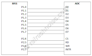
The following are the general pins in ADC.

D0 – D7: The digital data output pins. The converted data is accessed only when CS = 0 and RD is forced low.

CS: Chip select is an active low input used to activate the ADC chip.

RD: This is an input signal and is active low. RD is used to get the converted data out of the ADC chip. RD pin is also referred to as output enable (OE).

WR: This is an active low input used to inform the ADC to start the conversion process.

INTR: This is an output pin and is active low. It is a normally high pin and when the conversion is finished, it goes low to signal the CPU that the converted data is ready to be picked up.

Program to read temperature and put it on port 0.


ORG 0H
MOV P1, #0FFH ; make P1 as input port
CS BIT P2.4
READ BIT P2.5
WRITE BIT P2.6
INTR BIT P2.7
CLR CS ; CS = 0, chip enable
SETB INTR ; INTR = 1, clear end of conversion
BACK: CLR WRITE ; WR = 0, clear start conversion
SETB WRITE ; WR = 1 to start conversion
HERE: JB INTR, HERE ; wait for end of conversion
CLR READ ; conversion finished. Enable read
MOV A, P1 ; move data to accumulator
ACALL CONVERSION ; convert hex to DEC
ACALL DATA_DISPLAY ; Display it on port 0
SETB READ ; prepare for next round
SJMP BACK
; convert hex to dec (00 - FF to 000 - 255) and then to ASCII
ORG 300H
RAM_ADDR EQU 40H
CONVERSION:
HEX2DEC:
MOV R0, #RAM_ADDR
MOV B, #10
DIV AB ; divide by 10
MOV @R0, B ; save lower digit
INC R0
MOV B, #10v
DIV AB
MOV @R0, B ; save the next digit
INC R0
MOV @R0, A ; save last digit
RET
DATA_DISPLAY:
MOV R0, #RAM_ADDR
MOV P0, @R0
INC R0
ACALL DELAY
MOV P0, @R0
INC R0
ACALL DELAY
MOV P0, @R0
ACALL DELAY
RET
; some delay
DELAY: MOV R6, #50
HERE2: MOV R7, #255
HERE1: DJNZ R7, HERE1 ; stay until R7 = 0
DJNZ R6, HERE2 ; stay until R6 = 0
RET
END


Related topics:
8051 External Program Memory Interfacing   |   8051 External Data Memory Interfacing   |   8051 Memory Mapped IO   |   8051 LED Interfacing   |   8051 Switch Interfacing   |   8051 Keyboard Interfacing   |   8051 7-Segment Display Interfacing   |   8051 LCD Interfacing   |   8051 ADC Interfacing   |   8051 DAC Interfacing   |   8051 Relay Interfacing   |   8051 Stepper Motor Interfacing   |   8051 DC Motor Interfacing

List of topics: 8051

8051 Relay Interfacing

A relay is an electrically controllable switch widely used in industrial controls, automobiles, and appliances. It allows the isolation of two separate sections of a system with two different voltage sources. For example, a +5V system can be isolated from a 120V system by placing a relay between them. One such relay is called an electromechanical (or electromagnetic) relay (EMR).

8051 Relay Interfacing

Program to turns the lamp on and off by energizing and de-energizing the relay every second.

ORG 0H
MAIN:
SETB P1.0
MOV R5, #55
ACALL DELAY
CLR P1.0
MOV R5, #55
ACALL DELAY
SJMP MAIN
DELAY:
HERE1: MOV R2, #100
HERE2: MOV R3, #255
HERE3: DJNZ R3, HERE3
DJNZ R2, HERE2
DJNZ R5, HERE1
RET
END


Related topics:
8051 External Program Memory Interfacing   |   8051 External Data Memory Interfacing   |   8051 Memory Mapped IO   |   8051 LED Interfacing   |   8051 Switch Interfacing   |   8051 Keyboard Interfacing   |   8051 7-Segment Display Interfacing   |   8051 LCD Interfacing   |   8051 ADC Interfacing   |   8051 DAC Interfacing   |   8051 Sensor Interfacing   |   8051 Stepper Motor Interfacing   |   8051 DC Motor Interfacing

List of topics: 8051

8051 DAC Interfacing

Digital-to-Analog Converter (DAC) is a device widely used to convert digital pulses to analog signals. The number of data bit inputs decides the resolution of the DAC since the number of analog output levels is equal to 2”, where n is the number of data bit inputs. Therefore, an 8-input DAC provides 256 discrete voltage (or current) levels of output.

8051 DAC Interfacing

Let’s assume a 8-bit input DAC with reference voltage +5V and full scale output of 10V. Full-scale output of the DAC is achieved when all the data inputs of the DAC are high. The following equation is used to achieve full scale output. Vout = 5V + (5 * sin θ). To find the value sent to the DAC for various angles, we simply multiply the Vout voltage by 25.60 because there are 256 steps and full-scale Vout is 10 volts. Therefore, 256 steps /10 V = 25.6 steps per volt.

To generate sine wave, the following table is used to calculate DAC input.
Angle Magnitude Vout DAC Input
0 5 128
30° 0.5 7.5 192
60° 0.866 9.33 238
90° 1.0 10 255
120° 0.866 9.33 238
150° 0.5 7.5 192
180° 0 5 128
210° -0.5 2.5 64
240° -0.866 0.669 17
270° -1.0 0 0
300° -0.866 0.669 17
330° -0.5 2.5 64
360° 0 5 128

ORG 0H
COUNT EQU 13
AGAIN: MOV DPTR, #TABLE
MOV R2, #COUNT
BACK: CLR A
MOVC A, @A+DPTR
MOV P1, A
INC DPTR
DJNZ R2, BACK
SJMP AGAIN
ORG 300H
TABLE: DB 128, 192, 238, 255, 238, 192
DB 128, 64, 17, 0, 17, 64, 128
END


Related topics:
8051 External Program Memory Interfacing   |   8051 External Data Memory Interfacing   |   8051 Memory Mapped IO   |   8051 LED Interfacing   |   8051 Switch Interfacing   |   8051 Keyboard Interfacing   |   8051 7-Segment Display Interfacing   |   8051 LCD Interfacing   |   8051 ADC Interfacing   |   8051 Relay Interfacing   |   8051 Sensor Interfacing   |   8051 Stepper Motor Interfacing   |   8051 DC Motor Interfacing

List of topics: 8051

8051 ADC Interfacing

Analog-to-digital converters are among the most widely used devices for data acquisition. We need an analog-to-digital converter to translate the analog signals to digital numbers so that the microcontroller can read and process them. The ADC chips are either parallel or serial. In parallel ADC, we have 8 or more pins dedicated to bringing out the binary data, but in serial ADC we have only one pin for data out.

8051 ADC Interfacing - Parallel

The following are the general pins in ADC.
D0 – D7: The digital data output pins. The converted data is accessed only when CS = 0 and RD is forced low.

CS: Chip select is an active low input used to activate the ADC chip.

RD: This is an input signal and is active low. RD is used to get the converted data out of the ADC chip. RD pin is also referred to as output enable (OE).

WR: This is an active low input used to inform the ADC to start the conversion process.

INTR: This is an output pin and is active low. It is a normally high pin and when the conversion is finished, it goes low to signal the CPU that the converted data is ready to be picked up.

Reading Data from ADC:
Make CS = 0 and send a low-to-high pulse to pin WR to start the conversion.

Keep monitoring the INTR pin. If INTR is low, the conversion is finished and we can go to the next step. If INTR is high, keep polling until it goes low.

After the INTR has become low, we make CS = 0 and send a high-to-low pulse to the RD pin to get the data out of the ADC chip.

; main program
ORG 0H
MOV P1, #0FFH ; make P1 as input port
CS BIT P2.4
READ BIT P2.5
WRITE BIT P2.6
INTR BIT P2.7
CLR CS ; CS = 0, chip enable
SETB INTR ; INTR = 1, clear end of conversion
BACK: CLR WRITE ; WR = 0, clear start conversion
SETB WRITE ; WR = 1 to start conversion
HERE: JB INTR, HERE ; wait for end of conversion
CLR READ ; conversion finished. Enable read
MOV A, P1 ; move data to accumulator
ACALL CONVERSION ; convert hex to acsii
SETB READ ; prepare for next round
SJMP BACK
; convert hex to dec (00 - FF to 000 - 255) and then to ASCII
ORG 300H
RAM_ADDR EQU 40H
ASCII_RESULT EQU 50H
CONVERSION:
HEX2DEC:
MOV R0, #RAM_ADDR
MOV B, #10
DIV AB ; divide by 10
MOV @R0, B ; save lower digit
INC R0
MOV B, #10
DIV AB
MOV @R0, B ; save the next digit
INC R0
MOV @R0, A ; save last digit
DEC2ASCII:
MOV R0, #RAM_ADDR
MOV R1, #ASCII_RESULT
MOV R2, #3 ; digit count
REPEAT: MOV A, @R0
ORL A, #30H ; make it an ASCII digit
MOV @R1, A ; save it
INC R0
INC R1
DJNZ R2, REPEAT
RET
END


Serial ADC:
CS: Chip select is an active low input used to select the chip.

SCLK: Serial clock input. SCLK is used to bring data out and send in the control byte, one bit at a time.

DOUT: Serial data out. The digital data is clocked out one bit at a time on the H-to-L edge (falling edge) of SCLK.

DIN: Serial data in the control byte is clocked in one bit at a time on the L-to-H edge (rising edge) of SCLK.

STRB: Serial strobe output. In internal clock mode this indicates end-of-conver-sion. It goes high when the conversion is complete.

A control byte is fed into the ADC serially one bit at a time via the DIN pin with the help of SCLK. The control byte must be sent in with the MSB (most significant bit) going in first. The MSB of the control byte is high to indicate the start of the control byte.

When the last bit of the control byte is sent in the conversion starts, and STRB goes low. The end-of-conversion state is indicated by STRB going high. We can either wait or monitor STRB before we get the digital data out of the ADC chip.

The 8-bit converted digital data is brought out of the ADC via the DOUT pin using SCLK. As we apply a negative-edge pulse to the SCLK pin, the 8-bit digital data is read out one bit at a time with the MSB (D7) coming out first. The STRB goes high to indicate that the conversion is finished.

; program to adc data serially
ORG 0H
CS BIT P2.0
SCLK BIT P2.1
DIN BIT P2.2
DOUT BIT P2.3
MAIN: MOV A, #80H ; MSB = 1
MOV R3, #8 ; 8-bits
CLR CS ; CS = 0
; sending in control byte
SEND_BYTE:
RLC A ; give a bit to carry flag
MOV DIN, C ; send a bit to DIN
CLR SCLK ; SCLK low to high pulse
ACALL DELAY
SETB SCLK
ACALL DELAY
DJNZ R3, SEND_BYTE ; repeat for all 8-bits
SETB CS ; deselect ADC, start conversion
CLR SCLK ; SCLK = 0 during conversion
SETB DOUT ; make it an input
; reading data out
CLR CS ; CS = 0
SETB SCLK
ACALL DELAY
CLR SCLK ; first high to low
ACALL DELAY
MOV R3, #8
MOV A, #0H ; clear accumulator
READ_DATA:
SETB SCLK
ACALL DELAY
CLR SCLK ; high to low pulse to get bit out
ACALL DELAY
MOV C, DOUT ; move bit to carry flag
RLC A ; bring in the bit
DJNZ R3, READ_DATA ; read 8-bits
SETB CS ; cs = 1
MOV P1, A
SJMP MAIN
; some delay
DELAY: MOV R6, #50
HERE2: MOV R7, #255
HERE: DJNZ R7, HERE ; stay until R7 = 0
DJNZ R6, HERE2 ; stay until R6 = 0
RET
END


Related topics:
8051 External Program Memory Interfacing   |   8051 External Data Memory Interfacing   |   8051 Memory Mapped IO   |   8051 LED Interfacing   |   8051 Switch Interfacing   |   8051 Keyboard Interfacing   |   8051 7-Segment Display Interfacing   |   8051 LCD Interfacing   |   8051 DAC Interfacing   |   8051 Relay Interfacing   |   8051 Sensor Interfacing   |   8051 Stepper Motor Interfacing   |   8051 DC Motor Interfacing

List of topics: 8051

8051 LCD Interfacing

LCD can be used to display numbers, characters and graphics. Generally the following LCD pins are used to interface with 8051.

8051 LCD Interfacing

D0 – D7 (Data): The 8-bit data pins, DO – D7, are used to send information to the LCD or read the contents of the LCD’s internal registers.
RS (Register Select): There are two very important registers inside the LCD. The RS pin is used for their selection as follows. If RS = 0, the instruction command code register is selected, allowing the user to send a command such as clear display, cursor at home, etc. If RS = 1 the data register is selected, allowing the user to send data to be displayed on the LCD.

R/W (Read Write): R/W input allows the user to write information to the LCD or read information from it. R/W = 1 when reading; R/W = 0 when writing.

E (Enable): The enable pin is used by the LCD to latch information presented to its data pins. When data is supplied to data pins, a high-to-low pulse must be applied to this pin in order for the LCD to latch in the data present at the data pins.

Busy Flag: The busy flag is D7 and can be read when R/W = 1 and RS = 0, as follows: if R/W= 1, RS = 0. When D7 = 1 (busy flag = 1), the LCD is busy taking care of internal operations and will not accept any new information. When D7 = 0, the LCD is ready to receive new information.

To display letters and numbers, we send ASCII codes for the letters A – Z, a – z, and numbers 0 – 9 to data pins while making RS = 1.There are also instruction command codes that can be sent to the LCD. The command codes are in Hex.

Sending commands and data to LCD:
To send any of the commands to the LCD, make pin RS = 0. For data, make RS = 1. Then send a high-to-low pulse to the E pin to enable the internal latch of the LCD. Sending command and data using delay function.

ORG 0H
MOV A, #38H ; initialize LCD command. 2 lines, 5x7 dot matrix display
ACALL COMMWR ; call command write subroutine
ACALL DELAY ; give LCD some time
MOV A, #0EH ; display on, cursor on command
ACALL COMMWR ; call command write subroutine
ACALL DELAY ; give LCD some time
MOV A, #01H ; clear LCD command
ACALL COMMWR ; call command write subroutine
ACALL DELAY ; give LCD some time
MOV A, #06H ; shift cursor right command
ACALL COMMWR ; call command write subroutine
ACALL DELAY ; give LCD some time
MOV A, #84H ; cursor at line 1 position 4
ACALL COMMWR ; call command write subroutine
ACALL DELAY ; give LCD some time
MOV A, #'N' ; display letter N
ACALL DATAWR ; call data write subroutine
ACALL DELAY ; give LCD some time
MOV A, #'O' ; display letter O
ACALL DATAWR ; call data write subroutine
ACALL DELAY ; give LCD some time
AGAIN :SJMP AGAIN ; stay here
; send command to LCD
COMMWR:
MOV P1, A ; copy reg A to port 1
CLR P2.0; RS = 0 for command
CLR P2.1 ; R/W = 0 for write
SETB P2.2 ; E = 1 for high pulse
ACALL DELAY ; give LCD some time
CLR P2.2; E = 0 for high to low pulse
RET
; send data to LCD
DATAWR:
MOV P1, A ; copy reg A to port 1
SETB P2.0 ; RS = 1 for data
CLR P2.1 ; R/W = 0 for write
SETB P2.2 ; E = 1 for high pulse
ACALL DELAY ; give LCD some time
CLR P2.2 ; E = 0 for high to low pulse
RET
; some delay
DELAY:MOV R3, #50
HERE2:MOV R4, #255
HERE:DJNZ R4, HERE; stay until R4 = 0
DJNZ R3, HERE2 ; stay until R3 = 0v
RET
END

Sending command and data using busy flag and delay:
ORG 0H
MOV A, #38H ; initialize LCD command. 2 lines, 5x7 dot matrix display
ACALL COMMWR ; call command write subroutine
MOV A, #0EH ; display on, cursor on command
ACALL COMMWR ; call command write subroutine
MOV A, #01H ; clear LCD command
ACALL COMMWR ; call command write subroutine
MOV A, #06H ; shift cursor right command
ACALL COMMWR ; call command write subroutine
MOV A, #84H ; cursor at line 1 position 4
ACALL COMMWR ; call command write subroutine
MOV A, #'N' ; display letter N
ACALL DATAWR ; call data write subroutine
MOV A, #'O' ; display letter O
ACALL DATAWR ; call data write subroutine
AGAIN :SJMP AGAIN ; stay here
; send command to LCD
COMMWR:
ACALL READY; is LCD ready to receive command?
MOV P1, A ; copy reg A to port 1
CLR P2.0; RS = 0 for command
CLR P2.1 ; R/W = 0 for write
SETB P2.2 ; E = 1 for high pulse
ACALL DELAY ; give LCD some time
CLR P2.2; E = 0 for high to low pulse
RET
; send data to LCD
DATAWR:
ACALL READY; is LCD ready to receive data?
MOV P1, A ; copy reg A to port 1
SETB P2.0 ; RS = 1 for data
CLR P2.1 ; R/W = 0 for write
SETB P2.2 ; E = 1 for high pulse
ACALL DELAY ; give LCD some time
CLR P2.2 ; E = 0 for high to low pulse
RET
;read command register and check busy flag
READY: SETB P1.7 ; make p1.7 input port
CLR P2.0 ; RS = 0 access command register
SETB P2.1; R/W = 1 read command register
BACK: CLR P2.2 ; E = 0 for high to low pulse
ACALL DELAY ; give LCD some time
SETB P2.2 ; E = 1 for high pulse
JB P1.7, BACK ; stay until busy flag = 0
RET
; some delay
DELAY:MOV R3, #50
HERE2:MOV R4, #255
HERE:DJNZ R4, HERE; stay until R4 = 0
DJNZ R3, HERE2 ; stay until R3 = 0v
RET
END

Send string to LCD:
ORG 0H
MOV DPTR, #MYCMD
LOOP1:CLR A
MOVC A, @A+DPTR
ACALL COMMWR
ACALL DELAY
JZ SEND_DATA
INC DPTR
SJMP LOOP1
SEND_DATA:MOV DPTR, #MYDATA
LOOP2:CLR A
MOVC A, @A+DPTR
ACALL DATAWR
ACALL DELAY
JZ SEND_DATA
INC DPTR
JZ AGAIN
SJMP LOOP2
AGAIN :SJMP AGAIN ; stay here
; send command to LCD
COMMWR:
MOV P1, A ; copy reg A to port 1
CLR P2.0; RS = 0 for command
CLR P2.1 ; R/W = 0 for write
SETB P2.2 ; E = 1 for high pulse
ACALL DELAY ; give LCD some time
CLR P2.2; E = 0 for high to low pulse
RET
; send data to LCD
DATAWR:
MOV P1, A ; copy reg A to port 1
SETB P2.0 ; RS = 1 for data
CLR P2.1 ; R/W = 0 for write
SETB P2.2 ; E = 1 for high pulse
ACALL DELAY ; give LCD some time
CLR P2.2 ; E = 0 for high to low pulse
RET
; some delay
DELAY:MOV R3, #50
HERE2:MOV R4, #255
HERE:DJNZ R4, HERE; stay until R4 = 0
DJNZ R3, HERE2 ; stay until R3 = 0v
RET
ORG 300H
MYCMD:DB 38H, 0EH, 01, 06, 84H, 0
MYDATA:DB "HELLO0"
END


Related topics:
8051 External Program Memory Interfacing   |   8051 External Data Memory Interfacing   |   8051 Memory Mapped IO   |   8051 LED Interfacing   |   8051 Switch Interfacing   |   8051 Keyboard Interfacing   |   8051 7-Segment Display Interfacing   |   8051 ADC Interfacing   |   8051 DAC Interfacing   |   8051 Relay Interfacing   |   8051 Sensor Interfacing   |   8051 Stepper Motor Interfacing   |   8051 DC Motor Interfacing

List of topics: 8051
8051 7-Segment Display Interfacing

8051 7-Segment Display Interfacing

Program to display 1 on display 0 and 4 on display 1.

ORG 0H
AGAIN :
SETB P0.2 ; enable CS
CLR P0.1
CLR P0.0 ; enable display 0
MOV P1, #00000110B ; put pattern for 1 on display
CALL DELAY
SETB P0.0 ; enable display 0
MOV P1, #00101110B; put pattern for 4 on display
CALL DELAY
JMP AGAIN ; jump back to start
; a crude delay
DELAY:
MOV R0, #200
DJNZ R0, $
RET
END


Related topics:
8051 External Program Memory Interfacing   |   8051 External Data Memory Interfacing   |   8051 Memory Mapped IO   |   8051 LED Interfacing   |   8051 Switch Interfacing   |   8051 Keyboard Interfacing   |   8051 LCD Interfacing   |   8051 ADC Interfacing   |   8051 DAC Interfacing   |   8051 Relay Interfacing   |   8051 Sensor Interfacing   |   8051 Stepper Motor Interfacing   |   8051 DC Motor Interfacing

List of topics: 8051

8051 Keyboard Interfacing

Keyboards are organized in a matrix of rows and columns. When a key is pressed, a row and a column make a contact; otherwise, there is no connection between rows and columns.

The CPU accesses both rows and columns through ports; therefore, with two 8-bit ports, an 8 x 8 matrix of keys can be connected to a microprocessor. The rows are connected to an output port and the columns are connected to an input port.

8051 Keyboard Interfacing

To detect a pressed key, the microcontroller grounds all rows by providing 0 to the output latch, then it reads the columns. If the data read from the columns is D3 – DO = 1111, no key has been pressed and the process continues until a key press is detected. However, if one of the column bits has a zero, this means that a key press has occurred. For example, if D3 – DO = 1101, this means that a key in the Dl column has been pressed. After a key press is detected, the microcontroller will go through the process of identifying the key. Starting with the top row, the microcontroller grounds it by providing a low to row DO only; then it reads the columns. If the data read is all Is, no key in that row is activated and the process is moved to the next row. It grounds the next row, reads the columns, and checks for any zero. This process continues until the row is identified. After identification of the row in which the key has been pressed, the next task is to find out which column the pressed key belongs to. This should be easy since the microcontroller knows at any time which row and column are being accessed.
ORG 0H
MOV P2, #0FFH ; Make P2 an input port
KEYS1 :MOV P1, #0 ; make p1 as output port
MOV A, P2 ; read all columns ensure all keys are open
ANL A, #00001111B ; mask unused bits
CJNE A, #00001111B, KEYS1 ; check till all keys are released
KEYS2 :ACALL DELAY ; call 20ms delay
MOV A, P2 ; see if any key is pressed
ANL A, #00001111B ; mask unused bits
CJNE A, #00001111B, OVER ; key pressed, await closure
SJMP KEYS2
OVER :ACALL DELAY ; wait 20ms debounce time
MOV A, P2 ; check key closure
ANL A, #00001111B ; mask unused bits
CJNE A, #00001111B, OVER1 ; key pressed find row
SJMP KEYS2 ; if none, keep polling
OVER1 :MOV P1, #11111110B ; ground row 0
MOV A, P2 ; read all columns
ANL A, #00001111B ; mask unused bits
CJNE A, #00001111B, ROW_0 ; key row 0, find the column
MOV P1, #11111101B ; ground row 1
MOV A, P2 ; read all columns
ANL A, #00001111B ; mask unused bits
CJNE A, #00001111B, ROW_1 ; key row 1, find the column
MOV P1, #11111011B ; ground row 2
MOV A, P2 ; read all columns
ANL A, #00001111B ; mask unused bits
CJNE A, #00001111B, ROW_2 ; key row 2, find the column
MOV P1, #11110111B ; ground row 3
MOV A, P2 ; read all columns
ANL A, #00001111B ; mask unused bits
CJNE A, #00001111B, ROW_3 ; key row 3, find the column
LJMP KEYS2 ; if none, false input, repeat
ROW_0 :MOV DPTR, #KCODE0 ; set DPTR = start of row 0
SJMP FIND ; find column key belongs to
ROW_1 :MOV DPTR, #KCODE1 ; set DPTR = start of row 1
SJMP FIND ; find column key belongs to
ROW_2 :MOV DPTR, #KCODE2 ; set DPTR = start of row 2
SJMP FIND ; find column key belongs to
ROW_3 :MOV DPTR, #KCODE3 ; set DPTR = start of row 3
FIND :RRC A ; see if any CY bit is low
JNC MATCH ; if zero, get the ASCII code
INC DPTR ; point to next column address
SJMP FIND ; keep searching
MATCH :CLR A ; set A = 0, match is found
MOVC A, @A+DPTR ; get ASCII code from table
MOV P0, A ; display pressed key
LJMP KEYS1
; some delay
DELAY :MOV R3, #50
HERE2 :MOV R4, #255
HERE :DJNZ R4, HERE ; stay until R4 = 0
DJNZ R3, HERE2 ; stay until R3 = 0
RET
; ASCII look-up table for each row
ORG 300H
KCODE0 :DB '0','1','2','3' ; ROW 0
KCODE1 :DB '4','5','6','7' ; ROW 1
KCODE2 :DB '8','9','A','B' ; ROW 2
KCODE3 :DB 'C','D','E','F' ; ROW 3
END


Related topics:
8051 External Program Memory Interfacing   |   8051 External Data Memory Interfacing   |   8051 Memory Mapped IO   |   8051 LED Interfacing   |   8051 Switch Interfacing   |   8051 7-Segment Display Interfacing   |   8051 LCD Interfacing   |   8051 ADC Interfacing   |   8051 DAC Interfacing   |   8051 Relay Interfacing   |   8051 Sensor Interfacing   |   8051 Stepper Motor Interfacing   |   8051 DC Motor Interfacing

List of topics: 8051

8051 Switch Interfacing

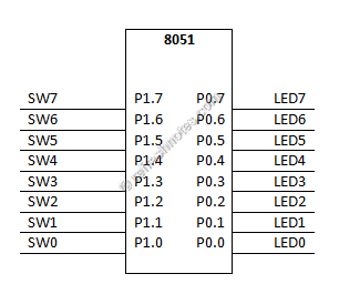
8051 port pins can be used to interface switch. We can monitor switch status through the IO pins.

8051 Switch Interfacing

Program to monitor switch status.
ORG 0H
MOV P1, #0FFH
MOV P0, #00H
AGAIN:
MOV P0, P1
SJMP AGAIN
END


Related topics:
8051 External Program Memory Interfacing   |   8051 External Data Memory Interfacing   |   8051 Memory Mapped IO   |   8051 LED Interfacing   |   8051 Keyboard Interfacing   |   8051 7-Segment Display Interfacing   |   8051 LCD Interfacing   |   8051 ADC Interfacing   |   8051 DAC Interfacing   |   8051 Relay Interfacing   |   8051 Sensor Interfacing   |   8051 Stepper Motor Interfacing   |   8051 DC Motor Interfacing

List of topics: 8051

8051 LED Interfacing

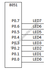
8051 port pins can be used to interface LED’s. We can control the LED by programming the IO pins.

8051 LED Interfacing

Program to toggle bits in 8255 output ports:
ORG 0H
MOV P0, 00H
MOV A, #55H
AGAIN:
MOV P0, A
ACALL DELAY
CPL A
SJMP AGAIN
DELAY:MOV R3, #100
HERE1:MOV R4, #255
HERE2:DJNZ R4, HERE2
DJNZ R3, HERE1
RET
END


Related topics:
8051 External Program Memory Interfacing   |   8051 External Data Memory Interfacing   |   8051 Memory Mapped IO   |   8051 Switch Interfacing   |   8051 Keyboard Interfacing   |   8051 7-Segment Display Interfacing   |   8051 LCD Interfacing   |   8051 ADC Interfacing   |   8051 DAC Interfacing   |   8051 Relay Interfacing   |   8051 Sensor Interfacing   |   8051 Stepper Motor Interfacing   |   8051 DC Motor Interfacing

List of topics: 8051
8051 Memory Mapped IO

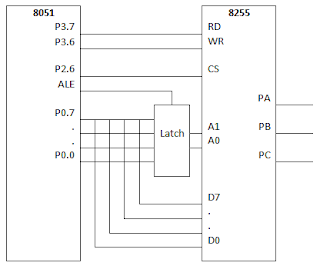
The 8255 chip, one of the most widely used I/O chips. It has three separately accessible 8-bit ports. The individual ports of the 8255 can be programmed to be input or output, and can be changed dynamically. The 8255 is programmed as a simple I/O port for connection with devices such as LCDs, stepper motors, and ADCs.

8051 Memory Mapped IO

As seen above, the 8255 is connected to an 8051 as if it is RAM memory. Notice the use of RD and WR signals. This method of connecting an I/O chip to a CPU is called memory-mapped I/O, since it is mapped into memory space. In other words, we use memory space to access I/O devices. For this reason we use instructions such as MOVX to access the 8255. For an 8255 connected to the 8051 we must also use the MOVX instruction to communicate with it.

8255 Port Selection:
CS A1 A0 Selection
1 0 0 Port A
1 0 1 Port B
1 1 0 Port C
1 1 1 Port D
0 x x 8255 is not selected

Address Lines:
4000H 4001H 4002H 4003H
A0 0 1 0 1
A1 0 0 1 1
A2 X X X X
A3 X X X X
A4 X X X X
A5 X X X X
A6 X X X X
A7 X X X X
A8 X X X X
A9 X X X X
A10 X X X X
A11 X X X X
A12 X X X X
A13 X X X X
A14 1 1 1 1
A15 X X X X

Program to toggle bits in 8255 output ports:
ORG 0H
MOV A, #80H ; configure ports as output
MOV DPTR, #4003H ; load control register address
MOVX @DPTR, A
MOV A, #55H
AGAIN :MOV DPTR, #4000H ; load port A address
MOVX @DPTR, A
INC DPTR ; load port B address
MOVX @DPTR, A
INC DPTR ; load port C address
MOVX @DPTR, A
CPL A ; toggle port bits
ACALL DELAY
SJMP AGAIN
DELAY :MOV R3, #50
HERE2 :MOV R4, #255
HERE :DJNZ R4, HERE ; stay until R4 = 0
DJNZ R3, HERE2; stay until R3 = 0
RET
END


Related topics:
8051 External Program Memory Interfacing   |   8051 External Data Memory Interfacing   |   8051 LED Interfacing   |   8051 Switch Interfacing   |   8051 Keyboard Interfacing   |   8051 7-Segment Display Interfacing   |   8051 LCD Interfacing   |   8051 ADC Interfacing   |   8051 DAC Interfacing   |   8051 Relay Interfacing   |   8051 Sensor Interfacing   |   8051 Stepper Motor Interfacing   |   8051 DC Motor Interfacing

List of topics: 8051
8051 External Data Memory Interfacing

8051 has 128K bytes of address space of which 64K bytes are set aside for program code and the other 64K bytes are set aside for data. Program space is accessed using the program counter (PC) to locate and fetch instructions, but the data memory space is accessed using the DPTR register and an instruction called MOVX, where X stands for external.

External Data ROM:
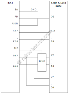
To connect the 8031/51 to external ROM containing data, we use RD. For the ROM containing the program code, PSEN is used to fetch the code. For the ROM containing data, the RD signal is used to fetch the data.

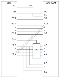
MOVX is a widely used instruction allowing access to external data memory space. To bring externally stored data into the CPU, we use the instruction “MOVX A, @DPTR”. This instruction will read the byte of data pointed to by register DPTR and store it in the accumulator. In writing data to external data RAM, we use the instruction “MOVX @DPTR, A” where the contents of register A are written to external RAM whose address is pointed to by the DPTR register.

8051 External Data Memory Interfacing - ROM

Read from External Data ROM:
ORG 0H
MYDATA EQU 1000H
COUNT EQU 30
MOV DPTR, #MYDATA ; point to data in external data ROM
MOV R2, #COUNT
AGAIN :MOVX A, @DPTR
MOV P1, A
INC DPTR
DJNZ R2, AGAIN
END


Copy from External Data ROM to Internal RAM:
ORG 0H
TABLE EQU 000H
RAMTABLE EQU 30H
COUNT EQU 10
MOV DPTR, #TABLE ; point to data in external data ROM
MOV R5, #COUNT
MOV R0, #RAMTABLE
AGAIN : MOVX A, @DPTR
MOV @R0, A
INC DPTR
INC R0
DJNZ R5, AGAIN
END


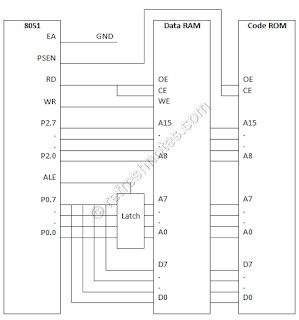
8051 with External Data and Program ROM:
8051 External Data Memory Interfacing - Program and Data ROM

Single External ROM for Program and Data:
8051 External Data Memory Interfacing - Single Program and Data ROM

A single external ROM chip is used for both program code and data storage. The space 0000H – 7FFFH is allocated to program code, and address space D000H – FFFFH is set aside for data. In accessing the data, we use the MOVX instruction. For accessing code, we use MOVC instruction.

External Data RAM:
8051 External Data Memory Interfacing - Data RAM

Read data from Port1 and store in external RAM:
ORG 0H
RAMDATA EQU 5000H
COUNT EQU 200
MOV DPTR, #RAMDATA ; point to data in external RAM
MOV R3, #COUNT
AGAIN :MOV A, P1
MOVX @DPTR, A
ACALL DELAY
INC DPTR
DJNZ R3, AGAIN
HERE : SJMP HERE
DELAY : MOV R5, 255
LOOP : DJNZ R5, LOOP
RET
END


External ROM and RAM:
8051 External Data Memory Interfacing - ROM and RAM

Memory more than 64KB:
In some applications we need a large amount (256K. bytes, for example) of memory to store data. However, the 8051 can support only 64K bytes of external data memory since DPTR is 16-bit. To solve this problem, we connect A0 – A15 of the 8051 directly to the external memory’s A0 – A15 pins, and use some of the PI pins to access the 64K-byte blocks inside the single 256Kx8 memory chip.
8051 External Data Memory Interfacing - More than 64K RAM


Related topics:
8051 External Program Memory Interfacing   |   8051 Memory Mapped IO   |   8051 LED Interfacing   |   8051 Switch Interfacing   |   8051 Keyboard Interfacing   |   8051 7-Segment Display Interfacing   |   8051 LCD Interfacing   |   8051 ADC Interfacing   |   8051 DAC Interfacing   |   8051 Relay Interfacing   |   8051 Sensor Interfacing   |   8051 Stepper Motor Interfacing   |   8051 DC Motor Interfacing

List of topics: 8051
8051 External Program Memory Interfacing

In 8051, we connect the EA pin to Vcc to indicate that the program code is stored in the microcontroller’s on-chip ROM. To indicate that the program code is stored in external ROM, this pin must be connected to GND.

8051 External Program Memory Interfacing

Port 0 & 2:
The PC (program counter) of the 8051 is 16-bit, it is capable of accessing up to 64K bytes of program code. In the 8051, port 0 and port 2 provide the 16-bit address to access external memory. Of these two ports, P0 provides the lower 8 bit addresses A0 – A7, and P2 provides the upper 8 bit addresses A8 – A15. More importantly, P0 is also used to provide the 8-bit data bus D0 – D7. In other words, pins P0.0 – P0.7 are used for both the address and data paths. This is called address/data multiplexing in chip design.

ALE:
ALE is an output pin for the 8051 microcontroller. ALE is used to select address or data path. It is important to note that normally ALE = 0, and P0 is used as a data bus, sending data out or bringing data in. Whenever the 8051 wants to use P0 as an address bus, it puts the addresses A0 – A7 on the P0 pins and activates ALE = 1 to indicate that P0 has the addresses.

PSEN:
PSEN is an output signal for the 8051 microcontroller and must be connected to the OE pin of a ROM containing the program code. In other words, to access external ROM containing program code, the 8051 uses the PSEN signal. The 8051 fetches opcode from external ROM by connecting PSEN pin to the OE pin of ROM.

Both Internal and External ROM:
In an 8051 system we could use the on-chip ROM for the boot code, and an external ROM will contain the user’s program. The system boot code resides on-chip and the user’s programs are downloaded into off-chip ROM. The system boot code resides on-chip and the user’s programs are downloaded into off-chip ROM. Upon reset the 8051 executes the on-chip program first; then, when it reaches the end of the on-chip ROM it switches to external ROM for the rest of the program code. System with both on-chip and off-chip ROM code where EA = Vcc, the controller fetches opcodes starting at address 0000, then goes on to address 0FFF (the last location of on-chip ROM). Then the program counter generates address 1000H and is automatically directed to the external ROM containing the program code.
8051 External Program Memory Interfacing

MOVC instruction is used to access the data located in program memory. The MOVC instruction, where C stands for code, indicates that data is located in the code space of the 8051.


Related topics:
8051 External Data Memory Interfacing   |   8051 Memory Mapped IO   |   8051 LED Interfacing   |   8051 Switch Interfacing   |   8051 Keyboard Interfacing   |   8051 7-Segment Display Interfacing   |   8051 LCD Interfacing   |   8051 ADC Interfacing   |   8051 DAC Interfacing   |   8051 Relay Interfacing   |   8051 Sensor Interfacing   |   8051 Stepper Motor Interfacing   |   8051 DC Motor Interfacing

List of topics: 8051